TI Nods to Smaller, More Efficient Satellites With GaN FET Gate Driver
Texas Instruments (TI) recently revealed a family of gallium nitride (GaN) FET gate drivers for space applications. Designed for satellite electrical power systems (EPS), these ICs are the so-called industry’s first space-grade GaN FET drivers that can support up to 200-V operation.

TI’s new space-grade GaN FET can support complex power systems for satellite computing needs.
Design Challenges of Satellite Electrical Power Systems
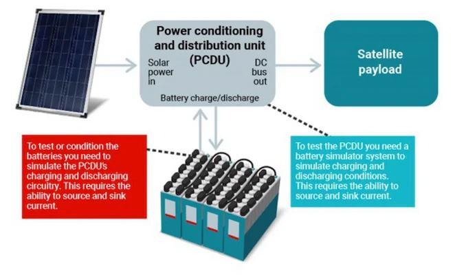
Satellite electrical power systems (EPS) consist of various subsystems, including solar panels, batteries, power conditioning and distribution units (PCDU), and backup power supplies. Satellite power architectures often employ synchronous buck, flyback, or full-bridge topologies.

Typical satellite electrical power systems (EPS) contain multiple components with individual functions.
These designs typically require PWM controllers and gate drivers to operate the MOSFETs or GaN FETs. To optimize the size, weight, and power (SWaP) of designs, satellite engineers require specialized gate driver ICs qualified for radiation tolerance, high frequency, efficiency, and current ratings. TI aims to meet these strict requirements with its new radiation-hardness-assured (RHA) ICs.
Space-Grade, High-Voltage FET Gate Drivers
The new family comes in two packaging options: the TPS7H60x5 series in plastic packaging and the previously available TPS7H60x3 series in ceramic packaging (datasheets linked). The GaN FET gate drivers support various voltage levels.
| Max Voltage | Recommended Operating Voltage | |
| TPS7H6005/TPS7H6003 | 200 V | 150 V |
| TPS7H6015/TPS7H6013 | 60 V | 45 V |
| TPS7H6025/TPS7H6023 | 22 V | 14 V |
All devices can handle a 1.3-A peak source current and 2.5-A peak sink current.
Each device can be operated in two modes: an independent input mode (IIM) and a PWM mode. The IIM allows each output to be controlled by its own input. The PWM mode generates two complementary outputs from a single input with adjustable dead time for each edge. The drivers have adjustable dead time, a 30-ns propagation delay, and 5.5 ns of typical delay matching. Internal LDOs can provide the 5-V drive voltage.
The plastic packages are outgas tested to ASTM E595 and are available in military temperature ranges (-55°C–125°C). TI has released accompanying support tools for the GaN FET gate drivers, including evaluation modules, reference designs, and simulation models.
GaN FETs Optimized for Space Missions
Developing electronics for space comes with unique constraints. Unlike terrestrial electronics, space electronics must be manufactured with radiation protection. This is especially true for satellites in low earth orbit (LEO) and geostationary orbit (GEO). The space environment is filled with radiation from trapped particles in the atmosphere caused by the sun and cosmic rays. These particles can cause temporary or permanent damage to electrical components.
NASA lists two main categories of radiation damage. Total ionizing dose (TID) is the long-term degradation of devices exposed to radiation, measured by resistance up to a certain krad(Si) dosage. Single-event effects (SEEs) are various individual events that can occur when ionized particles hit a device. This is noted by a linear energy transfer (LET) for destructive single-event effects (DSEE) measured in MeV cm2/mg. Space system designers need to select components that have been characterized to survive both the TID and DSEE profiles expected in their environments.
The new plastic TPS7H60x5 series is available in both radiation-hardened QMLP and radiation-tolerant space-enhanced plastic (SEP) grades. The QMLP devices (TPS7H60x5-SP) are rated for TID up to 100 krad(Si) and SEE free up to LET = 75 MeV-cm2/mg. The SEP devices (TPS7H60x5-SEP) are rated for TID up to 50 krad(Si) and SEE free up to LET = 43 MeV-cm2/mg.
Radiation Resilience and the SWaP Sweet Spot
Size, weight, and power (SWaP) are other important considerations for space missions. Launch providers have size constraints and can charge from $1,000 to $10,000 per kilogram, according to TI. This means the smaller the size and weight, the cheaper the mission. Satellites rely on solar panels for power generation. As such, batteries and panels often must occupy much of the size and weight budget allowed. Designers often strive to optimize SWaP as much as they can to extend mission lifetimes.

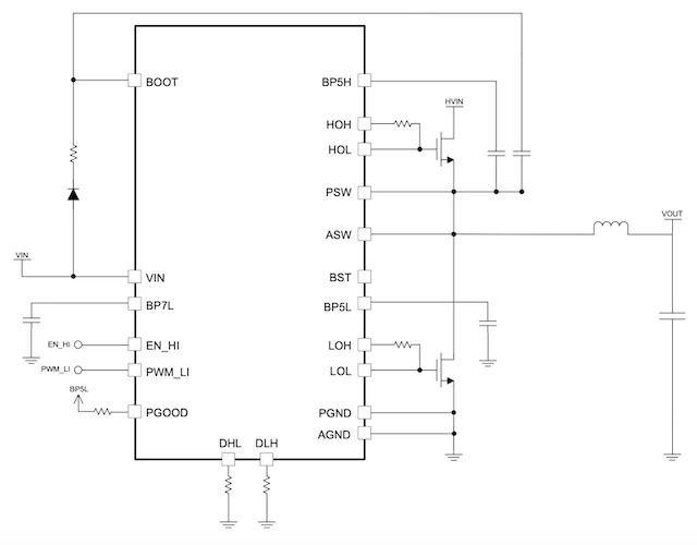
Simplified application diagram of the TPS7H60x5-SP and TPS7H60x5-SEP.
These considerations uniquely qualify GaN FETs for space, providing inherent radiation tolerance and smaller die size compared to typical silicon FETs. Gamma radiation, a source of permanent damage in space, can collide with the gate oxide layer of FETs and create “holes” in that layer. This results in voltage bias shifts that can degrade the performance of the transistor gate. GaN FETs do not have a gate oxide layer, making them less susceptible to this form of damage.
GaN is also a wide bandgap material, meaning that the drain-source distance can be made much smaller than silicon. These two features make GaN FETs—including TI's TPS7H60x5-SP/TPS7H60x5-SEP and TPS7H60x3-SP families—useful candidates for radiation hardness and smaller SWaP. aa
Sign up to our newsletter
Receive our latest updates about our products & promotions
