Exploring Microchip Technology’s Latest Innovations
In the fast-changing field of embedded systems and semiconductor technology, keeping up means using the newest hardware and software advancements. Microchip Technology’s February 2025 Product Roundup includes a carefully chosen set of the latest products, example designs, and software tools to help engineers and developers tackle today’s challenges.
This article will focus on these innovations, exploring their technical specifications, practical applications, and potential to advance embedded design. Focusing on power efficiency optimization, connectivity enhancement, and streamlined system integration, Microchip’s latest offerings provide engineers and developers with robust tools for complex projects.
Discrete mSiC MOSFET
Developed using Microchip’s mSiC technology—which exhibits elevated gate oxide and body diode reliability—the MSC750SMA140 is a 1,400-V, 750-mΩ silicon carbide N-channel MOSFET that is also available with an AEC-Q101-qualified option for automotive applications.
Designed with an optimized gate drive voltage range of 18–20 V to ensure robust switching characteristics, it achieves a reduced on-resistance of 750 mΩ for minimized conduction losses and improved power conversion efficiency.
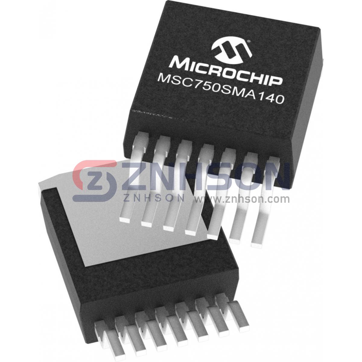
Engineered for high-temperature operation, the device (Figure 1) supports a maximum junction temperature rating of 175°C, enabling stable performance in thermally demanding environments. This mSiC MOSFET variant delivers enhanced thermal management and reliability, making it suitable for harsh operational conditions requiring sustained power handling and thermal resilience. Typical applications include photovoltaic inverters, power converters, industrial motor drives, hybrid-vehicle powertrains, EV chargers, and power supply and distribution.

Figure 1: The MSC750SMA140 mSiC power MOSFET (Source: Microchip Technology)
Housed in a TO-263 seven-lead XL package with a source sense pin for improved dynamic performance, the MSC750SMA140 achieves a low total gate charge (QG = 10.1 nC) and fast switching speed due to low internal gate resistance (ESR = 2.89 Ω). Other relevant dynamic characteristics include low-voltage rising and falling times, reduced turn-on/-off switching energy, and a short-circuit withstand time of 2.5 μs (VDS = 1,200 V, VGS = 20 V).
Because the gate drive power linearly depends on QG, a reduced charge lowers the power demand on the gate driver. This simplifies driver design, reduces component costs, and improves system compactness—critical for space-constrained applications such as automotive systems.
Additionally, a lower QG minimizes the energy required to charge and discharge the gate capacitance during switching transitions. This directly reduces switching losses, enabling higher-frequency operation without excessive power dissipation. For SiC MOSFETs, which excel in high-frequency/high-voltage applications (including EV traction inverters and solar inverters), this translates to improved efficiency and thermal management.
48V to 12V Power Conversion reference design
The automotive industry’s shift toward electrification has driven the adoption of 48-V electrical architectures, a response to the limitations of traditional 12-V systems in meeting modern efficiency, performance, and sustainability goals.
Despite the advantages of 48-V infrastructure—including reduced resistive losses and cable mass— vehicles continue to rely on a dual-voltage framework, retaining 12-V subsystems to power legacy electronics and ensure backward compatibility.
The 48-V to 12-V bidirectional DC/DC converter bridges the two domains, maintaining seamless operation of low-voltage components while preserving cost efficiency and simplifying the transition to next-generation electrified platforms.
The 48V to 12V Power Conversion reference design is a fully validated, ready-to-use platform built around the MIC2129, an AEC-Q100-qualified DC/DC stepdown synchronous controller. Supporting a broad input voltage range of 4.5 V to 100 V, the MIC2129 offers a selectable gate driver voltage feature, allowing users to choose between logic-level or standard MOSFETs. Additionally, the output voltage can be adjusted with a ±1% reference accuracy for precise regulation.
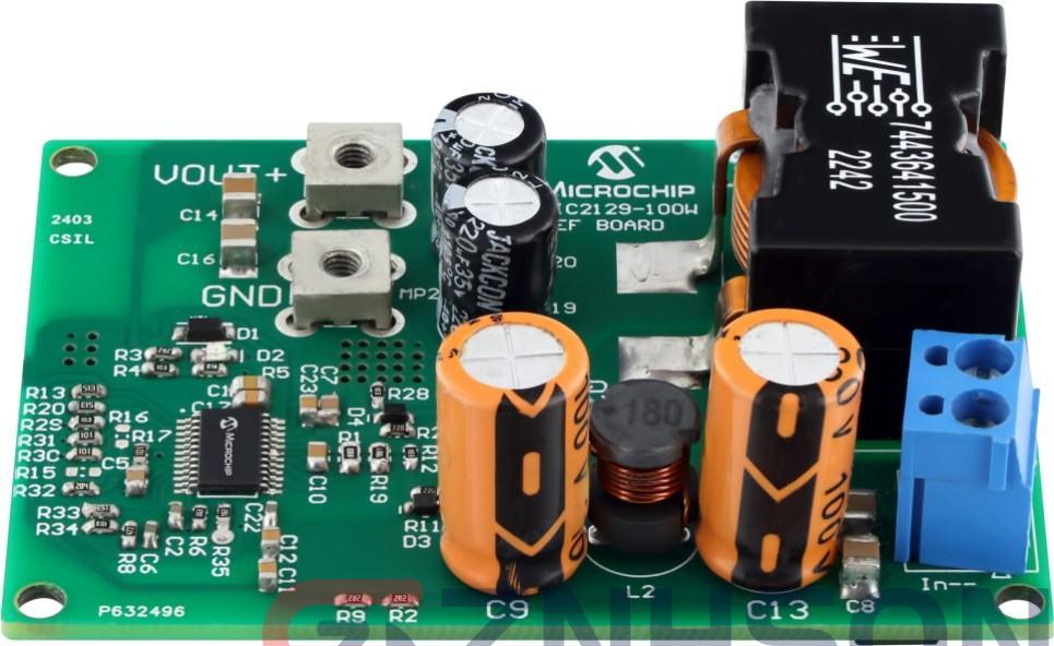
The RD24MIC2129 reference design (shown in Figure 2) employs a buck converter topology to deliver a 120-W constant-voltage and constant-current output. It efficiently steps down a 48-V input to a stable, 12-V output, supporting currents of up to 10 A. With an input voltage range of 18 V to 60 V, the design is also rated to handle DC voltages as high as 84 V for robust performance.
 Figure 2: A view of the reference design board (Source: Microchip Technology)
This reference design offers high-voltage, high-power, and high-efficiency power conversion solutions, specifically engineered for automotive, e-mobility, and EV applications, including EVs, e-scooters, and two- or three-wheeled systems. Optimizing power management efficiency significantly extends battery lifespan while ensuring operational safety through integrated protection mechanisms that proactively address potential operational risks.
Street Light Smart LED Driver reference design
LEDs are favored for street lighting due to high energy efficiency (50% to 70% savings), long lifespan (reducing maintenance), and brighter, directional light that enhances safety and cuts light pollution. They’re durable, integrate with smart controls, and meet regulations.
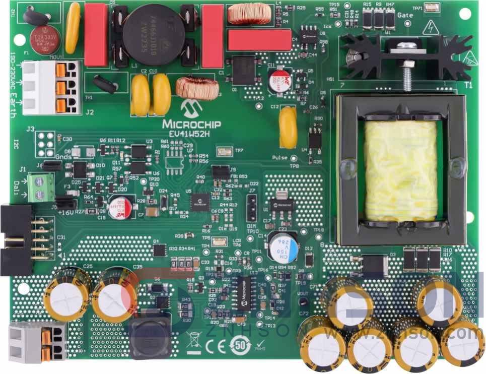
With more and more cities switching to energy-efficient LED lights, the streetlight market is poised for substantial expansion. Manufacturers of streetlights can save time and money by using Microchip’s LED Driver reference design (Figure 3).
In contrast to prefabricated alternatives, Microchip’s architecture allows for the customization of each driver to match the unique demands of different public bids. Manufacturers can adapt to the unique requirements of each town thanks to this personalization feature, which boosts their competitiveness and guarantees conformity with local rules and regulations.
 Figure 3: Upper view of Microchip’s Street Light Smart LED Driver reference design (Source: Microchip Technology)
The reference design accepts a broad input voltage range (190–265 VAC)—commonly 230 VAC—and delivers a maximum output power of 100 W with a high power factor of 0.99. It accommodates linear (analog) dimming, offering extensive amplitude control of the LED current, and PWM (digital) dimming, with a PWM pulse width as short as 150 ns.
The board is operable via a D4i-compliant interface. The D4i LED interface is specifically engineered to improve the functionalities of smart LED systems. It is an extension of the Digital Addressable Lighting Interface (DALI) protocol, extensively utilized for managing illumination in commercial and industrial environments. D4i incorporates the fundamental functionalities of DALI while enhancing its capabilities with additional features, including power monitoring and sophisticated energy management.
Additionally, the reference design incorporates protection features, including fault recovery with automatic retry delay, undervoltage detection of VDD and supply voltage (flyback output voltage), overvoltage detection of the LED load voltage (boost output voltage), and overcurrent detection of the load switch current.
This reference design, in conjunction with the Smart Street Light Controller Demonstration Application, enables users to establish comprehensive smart streetlight system demonstrations that include an LED driver, a smart streetlight controller, and industry-standard software protocols.
Sign up to our newsletter
Receive our latest updates about our products & promotions
